
Table of Contents
ToggleThe short version
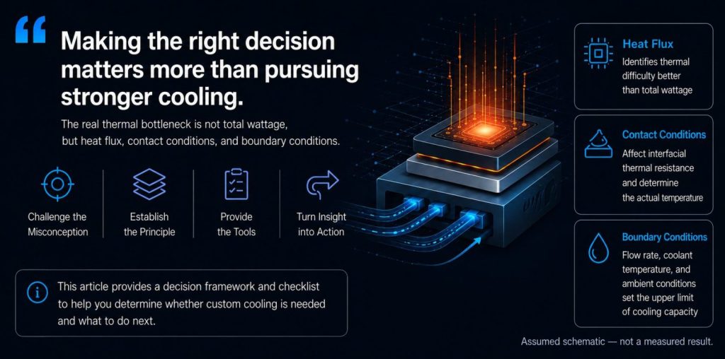
A defensible thermal assessment cannot rest on total wattage alone — it requires power and power distribution, effective heat-source area, TIM and contact conditions, package and thermal path, cooling boundary conditions, and allowable component or interface temperature.
- Total power is necessary but does not set difficulty. 200 W over 20 cm² is 10 W/cm²; the same 200 W on 1 cm² is 200 W/cm².
- Heat flux discriminates where wattage does not, but it is a signal, not a criterion — it does not point to an architecture.
- Contact conditions are the input most often missing. Using published specifications for one thermal interface material, bond line thickness alone moves the interface temperature difference from about 4 °C to about 33 °C at 100 W/cm².
- These six are inputs to an assessment, not its output.
By the time thermal becomes urgent, most of the expensive decisions have already been made. Tooling is committed. First silicon is scheduled. The fixture is on the machine. What remains is a narrow window in which someone has to decide whether the cooling approach will hold — usually without measured data, and usually against a date.
That pressure produces a specific question: how many watts can this cooling solution handle?
It is a reasonable question. It is also unanswerable in the form it is asked. What follows is the set of conditions that makes it answerable.
Total power is aggregate. Thermal failure is local.
Why "how many watts" has no defensible answer
The inference runs from total wattage to cooling architecture. It breaks at the first step.
Total power is a necessary input. Without it you cannot size a loop or estimate a fan curve. But necessary is not sufficient, and the reason is structural: total power is an aggregate quantity, while thermal failure is local.
A device fails because heat is generated in a specific place, concentrated over some area, and cannot leave quickly enough. None of that is contained in a board-level power number.
Take 200 W. Spread across a 20 cm² power module, that is 10 W/cm². Concentrated on a 1 cm² die, it is 200 W/cm² — a twentyfold difference in the quantity that governs the interface. Same wattage, different class of problem.
That comparison is only possible because both power and area were stated. Given wattage alone, even this much is unavailable, which leaves two possible responses: a range too wide to act on, or a confident number nobody can stand behind.
Heat flux is a better signal — and still not a criterion
To move from aggregate to local, the first useful quantity is heat flux.
Heat flux is the thermal power passing through a unit area, commonly expressed in W/cm². It describes not how much heat a system produces but how concentrated that heat is, which is why it discriminates thermal difficulty where total wattage does not.
It is still not a criterion.
Heat flux is a signal for identifying thermal risk, not a basis for selecting a cooling architecture — two devices at identical heat flux can require entirely different paths depending on package construction, contact conditions, and available volume.
What heat flux provides is a defensible sense of where a problem sits on the difficulty spectrum, and whether it warrants attention before commitment. That is useful. It is not an answer. Treating heat flux as the deciding number is the same error as treating wattage that way, in more technical dress.
The denominator: effective heat-source area vs package outline
When heat flux is computed incorrectly, the error is almost always in the denominator.
The common shortcut is to divide by the package outline. But the governing quantity is the effective heat-source area — the region where power is actually dissipated, typically the active area on the die, not the projected footprint of the package.
There is a layer in between. Heat travels toward lower resistance, so it spreads laterally through the lid, spreader, or substrate before reaching the next interface. By the time it arrives, the distribution is no longer what it was at the source.
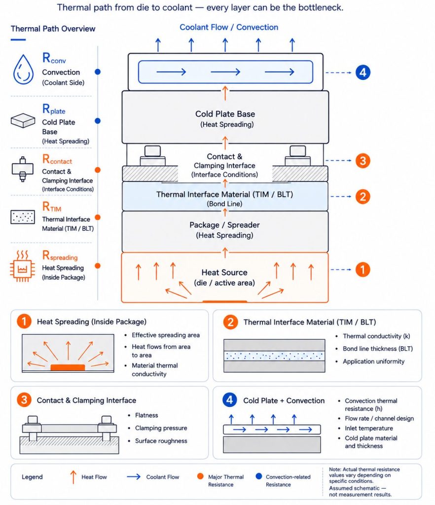
Dividing by the package outline therefore assumes that spreading has already distributed heat evenly across the whole package. For a single-die package with a well-designed spreader, that assumption is not badly wrong. It fails in two common cases:
- Multi-die packages, where power concentrates on a subset of dies while the package presents as one uniform block.
- Shared packages across a product family, where different SKUs use the same outline but contain very different die sizes.
The second case is not an edge case. TI’s application note on package thermal metrics measured this directly: for a tape-based area array chip scale package, junction-to-ambient resistance varies by nearly 8× across die size.
TI’s own guidance is that the figure must be re-measured or recalculated if a die shrink is planned.
A shared package is the same effect from the other direction. The outline does not change; the die inside it does — and the published number stops representing the part in front of you.
TI makes a broader point in the same document, and it is worth carrying beyond this one case: because test conditions have such a strong effect on measured values, any thermal resistance figure reported without its test conditions should be treated as suspect.
Spreading also has a cost, and is routinely overestimated. The 45° spreading assumption used as a rule of thumb is optimistic, and the deviation grows as the source gets smaller. The package outline is therefore not only the wrong denominator — it silently commits you to an assumption about spreading efficiency that may not hold.
Same wattage, very different problems
Put those together and a counterintuitive result follows: the higher-power system is not necessarily the harder one.
Scenario A — large-area power module. High total power, dissipated across a relatively large package. The mating surface is flat, mounting points and clamping force are specified, volume is available, coolant flow and inlet temperature are defined, and the temperature target carries margin. The wattage is intimidating; every segment of the thermal path is known. Difficult, but bounded.
Scenario B — small-area integrated SoC. Total power may be half of Scenario A or less, but it is concentrated on a small die. The package is thin, with limited room for lateral spreading. TIM selection and application are unspecified, and clamping force depends on how the unit was assembled. The module sits in an enclosure with no designed airflow path. The temperature target is tight.
Scenario B has the smaller number and the longer list of unknowns.
What is unclear is not the difficulty — it is the information. Scenario B is harder not because its physics are more severe, but because until those unknowns are closed, no one can state honestly whether it can be solved.
The six inputs a thermal assessment needs
At this point the conclusion is already visible: assessing thermal risk on a high-power device requires a set of conditions, not a single number.
The list below is the Thermal Risk Input Checklist — what is actually asked when scoping a problem. It is ordered by questioning sequence, not by physical thermal path. Heat physically travels from die to cooling end; in conversation, the first questions go to what you know best and what most often goes wrong.
| # | Input | What to provide | What breaks without it |
|---|---|---|---|
| 1 | Power and power distribution | Total power, how dissipation is distributed across the device, and whether it is steady-state or load-dependent | Total power alone cannot reveal local hot spots or transient behavior |
| 2 | Effective heat-source area | The area over which power is actually dissipated — not the package outline | Wrong denominator, wrong heat flux, wrong difficulty assessment |
| 3 | TIM, contact, and mounting conditions | TIM type, application or attach method, clamping torque, surface flatness, warpage | Contact resistance is the most frequently omitted segment and can dominate at high flux and small area; when it is unspecified, measured differences may not be attributable to the cooling solution at all |
| 4 | Package and thermal path | Die, substrate, spreader, and enclosure construction and materials; which directions heat can travel | Without the path, the limiting segment is unknown, and effort goes to the wrong place |
| 5 | Cooling boundary conditions | Available volume, airflow or flow rate, inlet temperature, allowable pressure drop, ambient conditions | Without boundary conditions, no statement about cooling capability holds |
| 6 | Allowable component or interface temperature | Junction limit, case or interface temperature target, who set it, and how much margin exists | Without a temperature target there is no criterion for “sufficient” |
These six are inputs to an assessment, not the output of one. Having them does not produce a cooling architecture — it converts “can this be solved” into “where does the risk sit, and what should be measured first.”
Contact conditions are the most frequently omitted
Of the six, contact conditions are the most frequently missing — and rarely in only one way.
- Selection without conditions. TIM chosen on bulk conductivity alone, without regard to how it behaves at the actual bond line thickness, pressure, flatness, and over service life.
- Clamping designed without a thermal requirement. Bond line thickness (BLT) becomes an assembly outcome rather than a design parameter, and unit-to-unit variation can exceed the improvement being pursued.
- “Thicker is safer.” The most intuitive, and the most common.
The third can be quantified — and from a published datasheet rather than an assumed value.
Bond line thickness changes the interface temperature difference
R″ = thickness ÷ conductivityArea-normalized bulk resistance of the layer≈ 4 °C
≈ 17 °C
≈ 33 °C
Condition: temperature differences are calculated at 100 W/cm² (= 1 W/mm²) using conduction through the material alone. Calculated using 6.0 W/(m·K) as the conservative conductivity basis. Published manufacturer data are not Hyper Cool Lab measurements.
Shin-Etsu X-23-7921-5 publishes three figures that need to be read together: thermal conductivity above 6.0 W/(m·K); interface thermal resistance below 7.0 mm²·K/W at 20 psi; and a bond line thickness of 25 μm at 20 psi.
Note the condition attached to the last two. The 25 μm is not a material property — it is a value that holds at a stated pressure. A mounting design that does not deliver that pressure does not deliver that BLT, and does not deliver the quoted interface resistance. A datasheet is not a guarantee; it is a set of figures that hold under conditions.
Area-normalized, the bulk resistance of the layer is thickness divided by conductivity:
- 25 μm → ≈ 4.2 mm²·K/W
- 100 μm → ≈ 16.7 mm²·K/W
- 200 μm → ≈ 33.3 mm²·K/W
Temperature difference follows directly, since ΔT equals area-normalized resistance multiplied by heat flux. At 100 W/cm² — that is, 1 W/mm² — the three cases give roughly 4 °C, 17 °C, and 33 °C. Same material, same die, separated only by whether thickness was controlled.
All three figures use the same basis: conduction through the material alone. That basis is worth stating, because it leaves something out.
TI uses the same relation to estimate interface resistance in its package thermal metrics note, and records the limitation explicitly: the estimate neglects the interfacial resistance that develops between any two surfaces. The three figures above describe the TIM layer, not the two faces where it meets metal.
The Shin-Etsu datasheet provides a second piece of information: under the stated condition of 20 psi, the interface thermal resistance is specified below 7.0 mm²·K/W. That quantity is not the same as the bulk resistance calculated from bond-line thickness and thermal conductivity alone.
Using 6.0 W/(m·K) as a conservative calculation basis, a 25 μm TIM layer has an area-normalized bulk resistance of no more than roughly 4.2 mm²·K/W. But because the conductivity is specified as a lower bound and the interface resistance as an upper bound, the two values cannot be directly subtracted and the difference called contact resistance.
The more useful conclusion is that thermal conductivity and BLT alone are not enough to predict actual interface resistance. Pressure, flatness, surface condition, and contact quality still affect the result. A TIM is a thermally conductive layer used to fill microscopic gaps and reduce interface resistance; once those gaps are adequately filled and reliable contact is maintained, excess bond-line thickness only adds bulk conduction resistance.
The same relation carries a second implication. Because ΔT scales with heat flux, identical BLT variation costs far less in a lower-flux system — at 25 W/cm², the spread from 25 μm to 200 μm is roughly 7 °C. Heat flux is what amplifies every other error.
These six inputs are not a hurdle placed in front of the person asking. They convert an unanswerable question into one that can be worked: where the risk sits, and what to measure first.
Three assumptions worth checking
High heat flux means liquid cooling. High flux means the problem warrants care. It does not point to an architecture. The same flux in a volume-rich, well-mounted system and in a space-constrained system with unspecified contact conditions lead to different reasonable next steps. Establish conditions, then discuss architecture; the reverse is guesswork.
Power and area are enough to choose an architecture. Heat flux resolves concentration only. Four inputs remain, and contact conditions in particular are often the segment that governs. A better cooling solution that produces no improvement usually indicates that the limiting segment was never at the cooling end, but somewhere between die and case.
The simulation already answered this. CFD, vendor tools, and AI-assisted analysis will produce a plausible result quickly. If that result is sufficient to justify the spend that follows, additional validation is not needed. It becomes necessary in three situations: when someone has to be accountable for the judgment, when the decision requires data behind it, or when machining and prototype spend is imminent and no controlled baseline exists. Simulation, datasheets, and generated recommendations occupy a specific position in the process — they are assumptions and test inputs. They indicate what to measure. They do not replace the measurement.
Before reading on, five questions:
- Of the six inputs, how many could you fill in right now?
- If someone asked for your effective heat-source area, would you give the die area or the package dimensions?
- Is your bond line thickness designed, or assembled?
- Is your current “temperature target missed” conclusion measured, or calculated?
- Before the next irreversible spend, do you have a controlled baseline to compare against?
What to do before asking for an assessment
Before asking anyone to assess a thermal problem, assemble the six inputs — including the ones that cannot yet be filled in.
The blanks are information. They indicate where risk is concentrated and what should be measured first.
With those in hand, fit and scope can be assessed: what class of problem this is, what data is missing, whether controlled measurement is warranted, and what a reasonable next step looks like.
Submit your thermal bottleneck
Tooling and silicon may already be committed. The next irreversible spend is not. Assemble the six inputs and we can assess fit and scope together — what class of problem this is, what data is missing, and what a reasonable next step looks like. This stage does not produce a cooling architecture recommendation.
Withholding an architecture recommendation isn't caution. Before anything is measured under controlled conditions, any architecture recommendation is a guess — just someone else's.
If you need a judgment with data behind it and a name attached to it, that requires a defined scope and evidence under stated conditions.
Frequently asked questions
How many watts can a cooling solution handle?
There is no defensible answer to that question on its own. Total power tells you how much heat must be moved, but not how concentrated it is, what path it takes, or what conditions it passes through. The same 200 W spread over 20 cm² is 10 W/cm²; concentrated on 1 cm² it is 200 W/cm² — a different class of problem. Six inputs are needed before difficulty can be assessed.
What is heat flux, and how is it calculated?
Heat flux is the thermal power passing through a unit area — total power divided by the effective heat-source area, commonly expressed in W/cm². The denominator is where it usually goes wrong: the effective heat-source area is where power is actually dissipated, typically the active area on the die, not the package outline.
Is thicker thermal interface material safer?
Not necessarily. Thicker is not inherently safer. Once the interface gaps are adequately filled and reliable contact is maintained, excess bond-line thickness adds bulk conduction resistance and increases the temperature drop across the TIM. A TIM’s conductivity is typically one to two orders of magnitude below the metals on either side of it; its function is to fill microscopic gaps, not to conduct. Provided the gap is filled and the material is not pumped out under pressure or thermal cycling, thinner gives lower interface resistance. Using published specifications for Shin-Etsu X-23-7921-5, bond line thickness alone moves the interface temperature difference from roughly 4 °C to roughly 33 °C at 100 W/cm².
Why can't thermal resistance figures be carried across packages?
Because the package outline does not represent the heat source. TI’s package thermal metrics note measured junction-to-ambient resistance varying by nearly 8× with die size for a tape-based area array chip scale package, and advises re-measuring or recalculating if a die shrink is planned. The same effect appears when a product family shares one package outline across very different die sizes. TI also notes more generally that any thermal resistance figure reported without its test conditions should be treated as suspect.
What information is needed before a thermal assessment?
Six inputs: power and power distribution, effective heat-source area, TIM and contact conditions, package and thermal path, cooling boundary conditions, and allowable component or interface temperature. These are inputs to an assessment, not its output — assembling them does not produce a cooling architecture, but it converts “can this be solved” into “where does the risk sit, and what should be measured first.” Blanks are useful: they show what to measure.
When a further assessment makes sense
This article covers what a thermal assessment needs as input. It does not cover the assessment itself, and the distinction matters enough to state plainly.
What this article can do for you: show what to assemble, what is missing, and what to measure first — turning “can this be solved” into a problem that can be described.
What it cannot do: tell you which cooling architecture your case needs, how many watts it can take, or whether air or liquid is the right path. Those require complete boundary conditions, measurement under controlled conditions, and someone accountable for the judgment.
Before you request an assessment
- I know the total power and roughly how it is distributed
- I can distinguish effective heat-source area from package outline
- I know which TIM is used and whether clamping force is specified
- I know which directions heat can travel
- I know the available volume, airflow or flow rate, and inlet temperature
- I know the allowable temperature limit and who set it
Six out of six is unusual. The blanks are what to measure next.
Three or four of six → submit your thermal bottleneck and we’ll assess fit and scope.
Almost none of six → start with Baseline Before Custom Cooling to see how controlled measurement fills the gaps.
Thermal work is rarely hard because the physics are hard. It is hard because the conditions are unstated.
So do not ask only how many watts a cooler can handle. State the conditions first — the answer only means something once the question does.
The next time someone asks how many watts a cooler can handle, the useful reply is another question: which kind of answer do you want — a guess, or one with conditions behind it?
References
- Shin-Etsu MicroSi, Thermal Interface Material X-23-7921-5 (Non-Solvent) Technical Data Sheet — thermal conductivity, interface resistance, and bond line thickness specifications
- Texas Instruments, Semiconductor and IC Package Thermal Metrics, SPRA953D (Rev. D, March 2024) — die size effect on junction-to-ambient resistance within a package, the significance of reported test conditions, and the stated limitation of the interface resistance estimate
- Electronics Cooling, The 45° Heat Spreading Angle – An Urban Legend? — applicability and deviation of the 45° spreading assumption
Note: figures cited above are published manufacturer and third-party data, not Hyper Cool Lab measurements. Refer to the current datasheet revision and your own test conditions for applicable values.